Research
Research
![]()
![]()
Semiconductors are the foundation of industries that underpin digital society, such as 5G, IoT, big data, autonomous driving, and smart cities. How can Japan, which led the semiconductor industry in decades previous, regain its standing? How can researchers make use of their knowledge to tackle the industry's revival as well as global issues? We asked Professor Hitoshi Wakabayashi and other leaders in charge of core technology development at the Integrated-Green-niX Consortium for Research and Human-Resource Development about their determination to find solutions and the technology that will make it possible.
In recent years, the global supply shortage of semiconductors has had a major impact on our lives, highlighting the importance of the semiconductor industry. In response to this social landscape, the government is now moving toward the revival of the Japanese semiconductor industry.
"The mass media is making a fuss, saying that Japan's semiconductor industry, which once dominated the world, has declined in the last 30 years. But even today, the world's semiconductor industry cannot exist without Japan. First of all, I would like to clear up the misunderstandings around that."
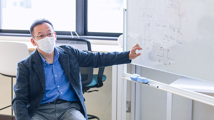
That's according to Hitoshi Wakabayashi, professor at Tokyo Institute of Technology's School of Engineering and Director of the Integrated Green-niX Consortium for Research and Human-Resource Development (iGX).
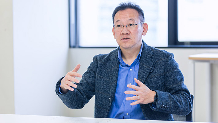
Director Hitoshi Wakabayashi
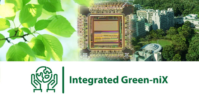
iGX is a new consortium adopted in April 2022 under the Initiative to Establish Next-generation Novel Integrated Circuits Centers (X-nics) by the Ministry of Education, Culture, Sports, Science and Technology, aiming to revive the Japanese semiconductor industry. Tokyo Institute of Technology, Toyohashi University of Technology, and Hiroshima University are collaborating with the aim of researching and developing innovative semiconductor integrated circuits and training experts who can manage them from a big picture perspective.
Wakabayashi continued: "Semiconductors come in a variety of types, including logic large-scale integrations (LSIs), memory, and sensors. In particular, most of the memory that temporarily stores data in computers and smartphones, the memory that stores your photos, and the image sensors installed in cameras are made in Japan. Japan has a dominating global market share of 40% to 50%. In addition, there are many markets related to semiconductor manufacturing equipment and materials in which Japanese companies dominate. Then why is the Japanese semiconductor industry said to have declined? This is because Japan is currently lagging behind Taiwan, South Korea, and the United States in terms of cutting-edge technology for logic LSIs, which serve as the command tower for semiconductors. Logic LSIs need to be miniaturized to increase processing speed and reduce power consumption, but there were no factories in Japan to develop and manufacture these states-of-the art LSIs. One of the reasons is that there has not been adequate investment in technology development. However, the Ministry of Economy, Trade and Industry (METI) is currently proposing investments of 10 trillion yen by the public and private sectors over the next 10 years. If all goes according to plan, it's not impossible that Japan will once again lead the world in the semiconductor industry."
As the miniaturization of electronic circuits moves forward, the performance of LSIs improves and the manufacturing cost per unit decreases. The circuit of the current state-of-the-art LSI is the 3 nanometer (a nano is one billionth) generation. In this context, METI has announced that it aims to establish next-generation semiconductor technology called "Beyond 2 Nano." The plan is that under METI, a research institute called the Leading-edge Semiconductor Technology Center (LSTC) and a new company called Rapidus will handle the technology development. Meanwhile, with the support of the Ministry of Education, Culture, Sports, Science and Technology, iGX aims to further advance the research and development of next-generation semiconductors. Moreover, the consortium is anticipating not only LSIs but also their fields of application, and it has its sights set on everything from research and development to implementation in a form that integrates memory, various sensors, and communication technology. As an educational institution, it also plans to make efforts to train experts who will lead the next-generation semiconductor industry.
"In addition, the name of the consortium (Integrated Green-niX) reflects the devotion of this consortium," says Wakabayashi. First of all, "integrated" refers to integrated circuit (LSI), and "green" means environmentally friendly. The X represents a cross-point of research and development for environmentally friendly next-generation semiconductors.
Wakabayashi added: "Green has a double meaning. The first is the development of manufacturing technology for eco-friendly next-generation LSIs, and the second is creating an eco-friendly world through the next-generation LSIs we have developed."
Developing next-generation LSIs will improve processing speed and reduce power consumption. However, cutting-edge EUV (extreme ultraviolet) exposure equipment is indispensable for further miniaturization of electronic circuits, and operating the exposure equipment requires an extremely large amount of power. Therefore, the consortium will focus on fields of application, such as how to create a green society using the next-generation LSIs it has developed, while developing eco-friendly manufacturing technology.
iGX is working on research topics that will greatly contribute to a green economy, such as integrated circuits/devices, semiconductor materials, sensors, edge LSIs, and network communications.
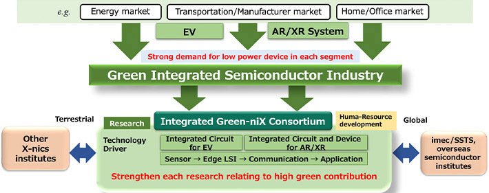
Research topics that iGX is pursuing
First up is 2D layered semiconductors, a next-generation semiconductor technology that Wakabayashi himself is working on. Currently, LSIs are fabricated on two-dimensional substrates. In principle, making them three-dimensional could improve performance without miniaturizing the circuit line width. Therefore, three-dimensional packaging is being promoted even in existing silicon semiconductors.
"However, if this increases the thickness of the substrate, the volume will increase. Therefore, by using a new 2D semiconductor material to replace silicon and make the substrate thin-film, 2D layered semiconductors can be used to achieve two-dimensions in a green way," according to Wakabayashi.
The new material is "transition metal dichalcogenide semiconductor transistor," which Wakabayashi has been researching and developing.
"Meanwhile, in order to verify the performance of these new materials, it is necessary to fabricate CMOS LSIs using semiconductor manufacturing equipment. Toyohashi University of Technology and Hiroshima University have fully equipped semiconductor manufacturing lines, so we plan to collaborate on research and development through this consortium," says Wakabayashi.
The consortium has two pillars in terms of applications for next-generation LSIs: cross reality (XR) and electric vehicles (EV).
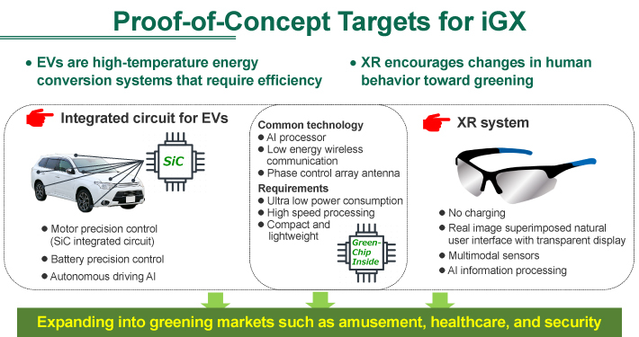
Devices that iGX amis to commercialize
First of all, XR is a general term for technology that complements the real world by fusing reality and virtual reality. Wearable devices such as smart glasses equipped with LSI play an important role as key devices for this purpose. Toyohashi University of Technology has been developing "intelligent biosensors" equipped with LSIs capable of sensing the environment. Breath sensors will become a core technology that contributes to drug efficacy and cancer markers. LSIs installed in smart glasses must be transparent, thin, and have high performance. Therefore, installing a 2D layered semiconductor will make it possible to include all the functions of modern smartphones. If the university can achieve this, it will be able to propose entirely new applications.
Research and development at Hiroshima University is focused on LSIs made from SiC (silicon carbide), which can operate in high-temperature environments such as those found in EV motors and nuclear power plants. By developing LSIs related to heat generation and temperature control, it will become a core technology that contributes to the efficiency of downstream operations such as smooth device control. Pushing forward the applications of both will advance the basic technology of high-speed communication and memory semiconductors.
Wakabayashi says that both of these technologies are in line with the goal of creating a green society using next-generation LSIs, so he believes that developing these application fields will coincide well with the collaboration of the three universities.
Further specific research and development details will be presented individually.
Furthermore, Wakabayashi advocates a "keep neutral scheme" for research and development at the consortium. "Keep neutral means avoiding being firmly aligned with any one company while engaging in industry-academia collaborative research. Since semiconductors are versatile and have a wide range of applications, the next-generation LSIs that we develop should not be limited to XR and EV, but rather be flexibly adapted to the needs and real-world issues of each era. However, if you are tightly bound to a specific company, the fields of application will be limited. Therefore, it is important for both us and the companies to ensure the flexibility to freely collaborate wherever and whenever necessary. On the other hand, we welcome collaborative research and development with companies on the premise of industry-academia cooperative research. Furthermore, we encourage collaborative research between companies and participating research institutions other than Tokyo Tech."
Finally, let's talk about human resource development at the consortium. The consortium aims to foster "LSI innovators." What kind of expert is this?
"As an example, the latest Apple computer today contains more than 100 billion transistors. That alone is surprising, but 40 years from now around 2060, they will likely contain a million times more transistors than that. In other words, the performance of a personal computer will have increased a million times compared to today. No one can imagine what kind of world that will bring about. Of course I can't imagine it either. However, it is the students of today who will build the future. For that reason, I would like students to think seriously about what kind of future they want to unlock, from a long-term perspective. And I hope that they will bring about innovation based on LSIs. That is the kind of LSI innovator that this consortium aims to foster."
For this reason, the university plans to set up an "Integrated Green-niX College" at the consortium to provide a comprehensive overview of the entire semiconductor value chain, and to train experts who will lead the next-generation semiconductor industry.
"Moving forward, industry, government, and academia will likely intensify efforts to revive the Japanese semiconductor industry. You can expect great things from iGX, as we will be playing a part in that," says Wakabayashi with enthusiasm.

One of the technologies for further improving the performance of LSIs is "three-dimensional packaging." This is an attempt to stack LSIs three-dimensionally. This makes the area smaller than when they are arranged side by side, and the wiring can be short. This achieves improved processing speed and reduced power consumption at the same time. Therefore, three-dimensional packaging is being promoted in existing silicon semiconductors.
A challenge worth noting is that although the area can be reduced by stacking, the thickness, and thus the volume, increases. Another major problem is heat buildup between LSIs, leading to a decline in performance.
In addition, next-generation silicon-based LSIs have a circuit line width of 2 nanometers as their ultimate goal. We face the problem of reduced electron mobility due to the consequent thinning of semiconductors.
Therefore, Wakabayashi's research group aims to create a next-generation LSI "2D layered semiconductor transistor" using a new material to replace silicon. The key material for this is transition metal dichalcogenide (TMDC) film transistor, which Wakabayashi has been developing for many years.
 Transition metal dichalcogenide (STEM image and schematic). The TMDC of the semiconductor device candidate material made of MoS2 is only 0.65 nanometers.
This is a semiconductor material composed of transition metals such as molybdenum (Mo) and tungsten (W) and chalcogens (group 16 elements) such as sulfur (S), selenium (Se) and tellurium (Te).
A feature of TMDC film is that it has a thin layered crystal structure. One layer is only 0.65 nanometers thick. Another thin layered material is graphene. Graphene is a single atomic layer of graphite that has been exfoliated. It is only one atom thick and has a flat, two-dimensional surface structure. Therefore, its electron mobility is very high, and it holds promise for use as a wiring material in place of copper in next-generation semiconductor devices. However, graphene has no bandgap (the width of the region where electrons cannot exist), making it difficult to use as a semiconductor material.
On the other hand, TMDC film has a bandgap and a flat surface like graphene, so electron mobility is much higher than in silicon.
Researchers also know that a monoatomic layer can be produced (like graphene) by methods like sputter deposition*1 and chemical vapor deposition (CVD)*2. Therefore, using TMDC film as a semiconductor material removes the need to create a three-dimensional structure. It promises to reduce the number of manufacturing processes, leading to lower manufacturing costs, as well as improved processing performance, smaller size, and lower power consumption.
Under iGX, Wakabayashi plans to develop not only LSIs but also new technologies based on TMDC film, such as power devices and displays.
The Hiroshima University Research Institute for Nanodevices (RIND) has been developing various types of semiconductor devices. In recent years, the institute has been focusing on the development of LSIs using silicon carbide (SiC) semiconductors. Compared to conventional silicon semiconductors, SiC semiconductors are characterized by resistance to high temperatures and radiation hardness. Whereas conventional silicon semiconductor LSIs do not operate normally when temperatures exceed approximately 120 ℃, SiC semiconductors operate at temperatures as high as 500 ℃ and do not malfunction even when subjected to large amounts of radiation. For this reason, NASA and other organizations around the world are conducting research and development aimed at installation in turbine engines of thermal power plants, automobiles, space probes with high radiation levels, nuclear power plants, nuclear fusion reactors, etc.
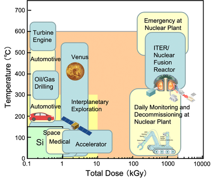
Industrial applications of SiC semiconductors. The vertical axis shows the operating temperature for each application, and the horizontal axis shows the required radiation resistance.
It should be noted that SiC power semiconductors are already installed in bullet trains and other vehicles. Power semiconductors are semiconductors that control and supply large amounts of power to motors and other devices. This application takes advantage of the characteristics of SiC semiconductors, which are resistant not only to high temperatures but also to high voltages. The US company Tesla was the first in the world to install SiC power semiconductors in an EV (Model 3). It achieves acceleration performance of 100km/h in 3.3 seconds. The fact that SiC semiconductors can operate at high temperatures likely contributes to this. However, no one has yet succeeded in putting SiC semiconductor LSIs into commercial use.
Professor Shin-Ichiro Kuroki of RIND commented: "SiC semiconductor LSIs will first be put into commercial use in fields where silicon semiconductors cannot be used, such as space probes and nuclear power plants. After that, their base will likely gradually spread to EVs."
At iGX, Hiroshima University is leading the research and development of LSIs using SiC semiconductors for the purpose of being installed in EVs.
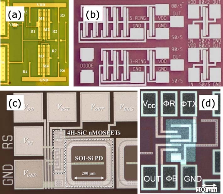
SiC integrated circuits for extreme environments under development. (a) SiC differential amplifier circuit (operates at 500 ℃), (b) SiC CMOS integrated circuit, SiC/Si-SOI hybrid CMOS pixel device, full SiC CMOS pixel device
"SiC power semiconductors installed in EVs can be operated at temperatures as high as 180 ℃. However, since conventional silicon semiconductors are used in addition to power semiconductors, a cooling system is essential to cool them down. However, if we could replace all semiconductors with SiC semiconductors, we would not need a cooling system, which would lead to a smaller and lighter car body, which would lead to greening," says Kuroki.
The Research Institute for Nanodevices (Hiroshima University), the Advanced Power Electronics Research Center (National Institute of Advanced Industrial Science and Technology (AIST)), and the Quantum Materials and Applications Research Center (Takasaki Advanced Radiation Research Institute, QST) are currently working together at iGX to develop SiC semiconductor LSIs with the aim of commercialization. The Research Institute for Nanodevices (Hiroshima University) conducts design and prototyping of various prototypes on the semiconductor manufacturing line; AIST's Advanced Power Electronics Research Center develops mass production technology for commercial use; and, QST's Quantum Materials and Applications Research Center plans to evaluate the performance of SiC semiconductors in terms of their resistance to radiation.
Kuroki expressed his enthusiasm. "Japan's economy has long been underpinned by heavy industry and the automobile industry. None of this is possible today without semiconductors. In particular, semiconductors will play an increasing role with the shift to electric vehicles and autonomous driving. However, Japan has been losing out to other countries in terms of business and investment in the semiconductor industry for the last 30 years. The semiconductor industry is a growth industry globally, so it is important for Japan to invest with a clear growth strategy. In particular, Japan's technological prowess in SiC semiconductors is in the top league, so we would like to work with everyone to develop it further at the world's research and development hub."
Since its founding in 1986, the Research Institute for Nanodevices (RIND) has consistently promoted research and development of LSI and device processes. In 1996, the name was changed to the Research Center for Nanodevices and Systems, but in 2008, together with the strengthening of medical-engineering collaboration, the name was changed to the Research Institute for Nanodevice and Bio Systems. In April 2022, the name was changed to the Research Institute for Nanodevices which continues to this day. The collaboration between medicine and engineering continues today, and since SiC semiconductors are particularly resistant to radiation, there is research and development underway of sensors to be installed in devices for new cancer treatment called boron neutron capture therapy.
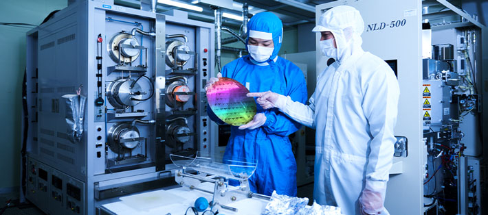
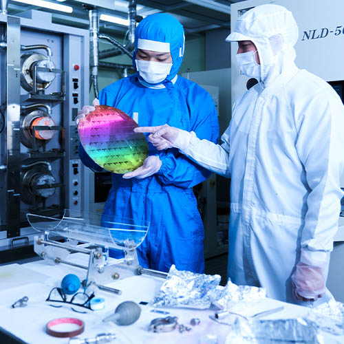
RIND Super Clean Room. It is possible to acquire integrated skills for everything from the fabrication of CMOS integrated circuits and device characteristics to measurement methods. Every year, we provide opportunities for middle and high school students to learn.
XR and EV are expected applications for next-generation LSIs. Next-generation wireless communication networks play an important role in both of these fields.
Professor Suguru Kameda of Hiroshima University believes that "Massive Connect IoT" will become mainstream in next-generation wireless communication networks.
IoT is an abbreviation for Internet of Things, which means that things directly exchange information with each other. Massive Connect IoT is a further evolution of that.
"The information sent and received by the devices underpinning the IoT society will be diversified. Smart glasses and EVs used for XR will also function as some of these devices. Furthermore, by using AI to analyze large amounts of data obtained from a huge number of devices, such as sensors and cameras all over the city, the network itself will have intelligence and evolve to create new value. In this context, wireless communication networks will not only be used for smartphones, but will also interact with electric, transportation, and all other types of networks, becoming sophisticated social infrastructure that underpins our lives," according to Kameda.
For example, 5G is the latest mobile communication system currently used for devices such as smartphones, but 6G is scheduled to enter commercial use around 2030. The three functions required for 6G are (1) ultra fast and large capacity, (2) ultra-low latency, and (3) ultra numerous connectivity.
Kameda has therefore been researching "ultra numerous connectivity." This technology efficiently exchanges a large amount of information transmitted by a huge number of devices on a network.
"I started this research after the Great East Japan Earthquake in 2011. At the time, Sendai (location of Tohoku University where I was enrolled) was affected by the disaster, and I went into crisis mode when the network was congested and mobile phones had no connection. Furthermore, in an IoT society, the amount of information exchanged between devices is expected to increase exponentially even in normal times, so we proposed the idea of Massive Connect IoT."

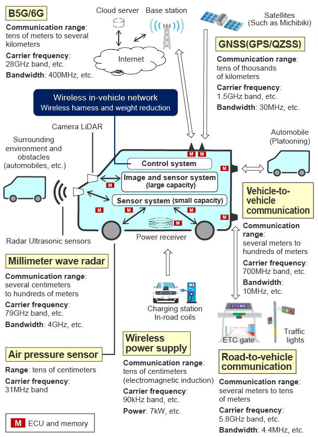
An information network for automobiles and traffic achieved by Massive Connect IoT. A wide variety of wireless technologies are being used even for just automobiles.
What kind of challenges is iGX actually tackling? There are two types of information flow in wireless communication: uplink and downlink. Uplink is transmissions from multiple devices to one base station, and downlink is transmissions from one base station to multiple devices.
"Prince Shotoku*3 is said to have been able to listen to 10 people at once, and that's exactly what uplink can do. Uplink is a more difficult technology than downlink. Downlink has had a greater amount of information (for example, watching YouTube videos on a smartphone), but in the future there will be more opportunities to transmit information from devices, so uplink will have increasing amounts of information. Therefore, I am particularly focusing on research on how to efficiently transmit and receive uplink information."
Kameda singled out "space-time synchronization". With uplink, all devices transmit information separately. In response, the base station sends signals to the devices to control the timing of transmissions. However, the problem here is that the different distances from each device to the base station cause a time lag in the arrival of signals from each device. Space-time synchronization solves this problem of time and distance (space). By finely controlling the transmission times according to the distance from the device to the base station, all devices will perform wireless communication efficiently.
Kameda's goal with iGX is to establish a massive concurrent connection technology using space-time synchronization. Kameda says he will continue to push forward with R&D with the aim of implementing this technology in next-generation wireless communication networks in the near future.
*3 Prince Shotoku: a member of the imperial family of Japan in the seventh century. Legend has it that when ten people vying for him to hear their petitions all talked at once, he understood all the words uttered by each person and was able to give an appropriate reply to each.

As the amount of digital data is expected to increase more and more, there is a demand for LSIs with even higher processing speeds and smaller sizes. To that end, it is essential to improve the performance of the memory that stores data.
To begin with, there are various types of memory. Depending on the required performance, they are divided into layers as shown in the figure below.
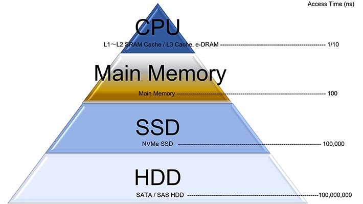
Diagram showing memory hierarchy
First of all, the top layer is for the CPU, which has a small capacity but requires ultra-high-speed processing. Memory called SRAM is used here. In contrast, the lowest layer is called storage (auxiliary storage device), which has low processing speed but large capacity and low cost. HDDs and SSDs are used here. And in the middle is a layer called main memory (main storage device). For example, when watching a video on a computer or smartphone, the video is temporarily saved in the built-in main memory, and the data is read out and played back. Currently, DRAM is primarily used for main memory. However, as the amount of data continues to rapidly increase, DRAM is approaching its physical limits in terms of achieving both large capacity and miniaturization.
"Therefore, research into replacing DRAM with ferroelectric memory (FeRAM) as the main memory is the main theme of my research group at iGX. Insulator materials are used for DRAM, but FeRAM uses ferroelectrics instead of insulators, so it is possible to increase the density of the device, significantly increase capacity, and reduce size," states Associate Professor Kuniyuki Kakushima.
FeRAM is a non-volatile memory that can read and write data by applying external voltage and does not lose data even when the power is turned off. In addition to achieving both large capacity and miniaturization, FeRAM also features low power consumption. "There are two ways to read and write memory data, one that uses current and one that uses voltage. The one that uses voltage consumes significantly less power. DRAM uses voltage, but it is volatile, which means data is lost when the power is turned off. On the other hand, FeRAM uses voltage and is non-volatile, meaning that data is not lost even when the power is turned off, so it consumes very little power," explains Kakushima.
In fact, FeRAM is familiar to us. FeRAM is installed in contactless IC cards (RFIDs), such as Suica used in Japan's transportation system, so it has already been in commercial use for a long time. However, these devices use a material such as lead zirconate titanate (PZT), which is a factor hindering the miniaturization of FeRAM. If you try to decrease the film thickness of PZT in order to miniaturize the device, you will lose the properties of ferroelectrics. Therefore, materials researchers are searching for alternative materials to PZT. One of them is a ferroelectric called aluminum scandium nitride (AlScN). Therefore, Kakushima and colleagues are working to develop FeRAM that uses AlScN.
AlScN has an asymmetric crystal structure. Kakushima states: "There are several substances with asymmetric crystal structures, but there are few substances whose crystal structure does not break even when voltage is applied, and AlScN is one of them."
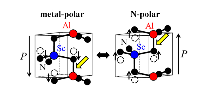
Schematic diagram of aluminum scandium nitride ferroelectrics. AlScN has an asymmetric crystal structure. Large spheres represent Al or Sc, and small spheres represent N. Since N is negatively charged, the crystal structure flips 180 degrees when an external voltage is applied. In other words, the state on the left and the state on the right are interchanged. That makes it possible to represent the 0s and 1s of data. Since these two states are stable, they are also non-volatile, which means that data is not lost even when the power is turned off.
However, even if the AlScN thin film exhibits excellent properties, the properties of the device change as voltage is repeatedly applied. Therefore, Kakushima and colleagues fabricated an AlScN memory chip using a thin film manufacturing method called atomic layer deposition (ALD) and sputter deposition, which are actually used in the manufacture of semiconductor devices. They are conducting experiments to observe how the properties of the device change by repeatedly applying voltage. "We have almost fully identified the factors that cause the properties to change, and we are currently focusing on R&D of technologies to reduce changes in properties," explains Kakushima.
For the commercial use of next-generation FeRAM, it is very important to ensure the reliability of not only the material but also the product. Through iGX, Kakushima is interacting with researchers and companies in different fields, aiming to put the technology into commercial use as soon as possible.
LSIs are increasingly required to process large amounts of data at high speed using AI. Under these circumstances, development is underway of a rewritable LSI, called a field-programmable gate array (FPGA), that is fit for AI.
An FPGA stands out for allowing the user to freely reconfigure the circuit according to the application. With the rapid spread of AI in recent years, Associate Professor Hiroki Nakahara (Tokyo Institute of Technology) is working on the development of FPGA implementation technology that is optimal for AI deep learning and machine learning, as well as design methods and tools for AI to efficiently process data using an FPGA.
"Currently, AI data processing capacity is doubling per year. If this capacity increases by ten times its current value, it will perhaps be on par with the human brain.[Ref. 1] I expect that it will become reality within three to four years," said Nakahara.
Pursuing this, in recent years there has been robust research and development of dedicated AI CPUs.
Nakahara continues, "AI processing makes predictions by repeating multiply-accumulate operations one trillion or ten trillion times on input data while reading training data. Therefore, increasing the number of memories to store more training data and increasing the number of multiply-accumulate operation circuits inside the CPU improve the processing power of AI. However, the amount of data processed by AI has increased dramatically, and in order to process it in real time, we have no choice but to increase the number of arithmetic circuits, and the scale of CPUs tends to increase."
Instead of relying on existing CPUs, Nakahara focused on the flexibility of FPGAs, which allow the circuits to be freely rewritten. He developed a calculation method that can express the values "-1", "0" and "1" with 2 bits. Based on this, he invented a technology that can express in 2 bits calculations that required 32 bits with conventional CPUs. As a result, by implementing a circuit dedicated to ternary operations on the FPGA, he was able to significantly reduce the size without degrading the processing performance of the AI.
"Many attempts have been made in Japan and overseas to reduce the number of bits, but usually reducing the number of bits reduces the recognition performance of AI. However, my laboratory has technology to limit the deterioration of recognition performance, and that is our strength," states Nakahara.
He is also conducting research to reduce the amount of calculations of AI itself.
"AI processing is an addition and multiplication monster. Therefore, we are creating a dictionary to store the data, and store the calculation results in advance. As a result, calculations can be completed simply by referencing the dictionary, greatly reducing the amount of calculations. We were also able to overcome the problem of increasing the size of the dictionary by using ternary operations," explains Nakahara.
The figure below shows an FPGA with multiple dictionaries (the part labeled "CLB"). Which dictionaries to refer to and in what order can be set using a program. The advantage of FPGA is thus that an LSI circuit can be freely designed and changed according to the application.
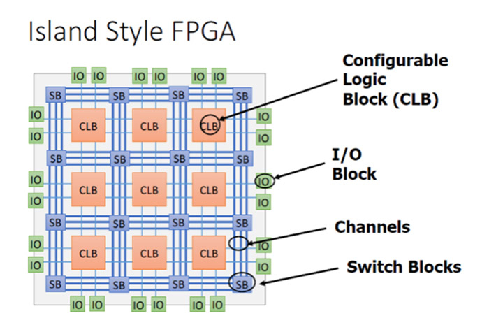
Configuration of a typical FPGA. The configurable logic block (CLB) functions as a dictionary that stores data. A large number of CLBs are arranged in an island pattern, and connectable wiring surrounds the periphery of the CLBs. By configuring the wiring according to the design using a program that rewrites the FPGA, it is possible to set which CLBs are to be referenced and in what order.
"Even if AI evolves further moving forward, we can deal with it by simply rewriting the FPGA as necessary. FPGAs and AI are seemingly very compatible," says Nakahara. In addition to the dictionary reference method, an algorithm called "pruning" is introduced to reduce unnecessary operations, which both improves processing speed and also reduces power consumption.
The strength of Nakahara's research group is thus that it is involved with everything from the development of theory and algorithms to circuit design to create them and implementation on FPGAs.
Leveraging this strength, Nakahara established the Tokyo Tech start-up Tokyo Artisan Intelligence (TAI) in March 2020. Currently, the company is engaged in the AI system implementation business using FPGA.
Nakahara describes, "currently, there is a growing need for cost reduction and safety improvement using AI image processing. TAI is promoting the introduction of AI in collaboration with customers in a wide range of fields, such as increasing productivity due to labor shortages in primary industries such as fisheries, preventing accidents at work sites, medical care, healthcare, and nursing care."
For example, in 2020, through joint development with Maruha Nichiro, we succeeded in reducing human error and cutting costs by automating the number of farmed fish using AI image processing.[Ref. 2]
In addition, TAI is also moving forward with its project of mass-producing FPGA systems for AI processing, aiming for a 2023 release.
Improving the efficiency of AI calculation processing is indispensable in iGX's application fields of XR and EV. Therefore, Nakahara will continue to deepen exchanges with researchers and companies in various fields participating in the consortium, and plans to build a highly versatile next-generation FPGA platform that can be used to meet a wide range of needs.
One of the key devices for achieving cross reality (XR) is smart glasses. Sensors installed in the glasses automatically sense the ambient information, visualize useful information for us, and display it in real space through the lenses.
Toyohashi University of Technology has been researching and developing "intelligent biochips" equipped with LSIs. Professor Kazuaki Sawada describes their features as follows. "Currently, biosensors that measure the concentration of viruses and red blood cells in blood are widely used in medical settings. However, existing biosensors are mounted on plastic substrates, and the data acquired is transferred to a personal computer for analysis. Meanwhile, the intelligent biochip we are developing has both sensors and a CMOS integrated circuit (LSI) on a silicon chip. That makes it possible to do analysis on the spot (i.e., without transferring data) at high speed and with low power consumption."
The development of intelligent biochips requires materials, structures, and manufacturing processes not employed for conventional silicon semiconductors, so they cannot be manufactured on existing silicon semiconductor manufacturing lines. On the other hand, Toyohashi University of Technology's Electronics-Inspired Interdisciplinary Research Institute (EIIRIS) has a semiconductor manufacturing line that can freely prototype semiconductors with new principles, structures, and materials. Students can design, fabricate, and evaluate LSIs. That makes it possible to fabricate this kind of biochip. Therefore, iGX has started research and development of a "multimodal sensor chip" that further develops this intelligent biochip and expands its range of applications. The plan is to install it in smart glasses.
"A multimodal sensor chip is a single chip that combines a chemical sensor that detects environmental pollutants such as toxic gases and pathogens such as viruses, a physical sensor that detects wind speed, sound waves, vibrations, etc., and an LSI. Simultaneously sensing various types of information and analyzing the data using artificial intelligence should make it possible to detect early signs of disaster and disease and clarify unexpected causal relationships," according to Sawada.
For example, landslide prediction is currently based on rainfall. However, if a device can simultaneously sense the smell of a river, changes in water quality, wind speed, etc., the accuracy of landslide prediction will be improved. It may also lead to the discovery of previously unknown signs. It is conceivable that by constantly sensing multiple types of substances contained in exhaled breath with smart glasses, we will detect subtle changes and discover diseases such as cancer at an early stage.
Sawada plans to incorporate several hundred types of sensors and LSIs into a single chip over the next 10 years. He says that by doing so, he and his team hope to enable various types of 'predictive sensing' and help create a world that is environmentally friendly, safe, and secure.
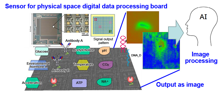
Conceptual diagram of multimodal sensor. Multiple sensors and LSIs are mounted on a single chip to create a new sensing application.
Toyohashi University of Technology is a national university founded in 1976. At that time, Japan was in the midst of rapid economic growth, and was taking the world by storm in the semiconductor industry. However, because there was not enough education on semiconductors at the university, the former Ministry of Education, Science, Sports and Culture took the initiative in conceptualizing and setting up the predecessor of the Electronics-Inspired Interdisciplinary Research Institute (EIIRIS) at Toyohashi University of Technology. At that time, the LSI manufacturing line at NEC's Tamagawa plant was relocated and rebuilt so that students could learn the semiconductor manufacturing process in earnest. About two-thirds of the professors came from the semiconductor industry. This provided students with an environment in which they could directly acquire the real skills of the semiconductor industry. "Our university has made efforts to cultivate experts who understand the overall picture of the semiconductor industry. This idea is consistent with the human resource development concept at iGX," explains Sawada.
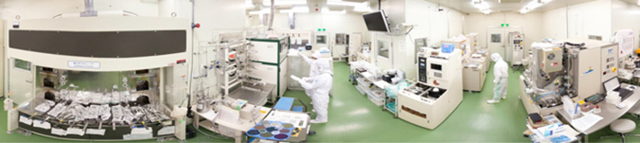
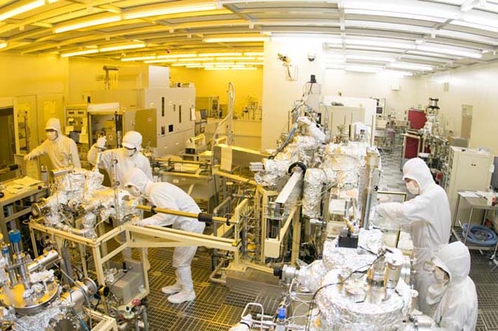
LSI plant at Toyohashi University of Technology (R&D facility):A facility capable of the integrated design, manufacture, and evaluation of LSIs that combine CMOS and sensors. Students master on their own the equipment and acquire the general skills necessary for semiconductor manufacturing, including maintenance of the semiconductor facility.

The Special Topics component of the Tokyo Tech Website shines a spotlight on recent developments in research and education, achievements of its community members, and special events and news from the Institute.
Past features can be viewed in the Special Topics Gallery.
Published: February 2023


![]()
© Tokyo Institute of Technology. All rights reserved.
![]()